
 English
  Español
  Deutsch
Content
What a Metallographic Microscope Delivers
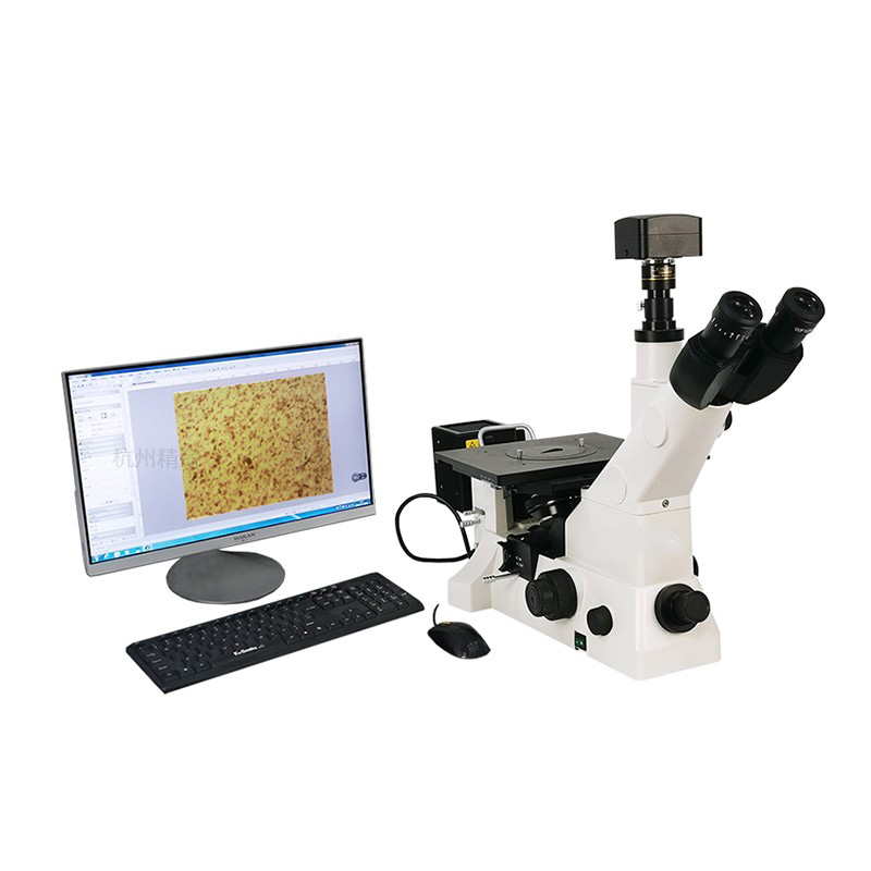
A metallographic microscope is an optical instrument designed specifically for examining the microstructure of metals and alloys through reflected light illumination. Unlike biological microscopes that transmit light through transparent specimens, metallographic systems direct light onto a polished metal surface and capture the reflected image. These instruments typically achieve magnifications ranging from 50x to 1000x, with a practical resolution limit of approximately 0.2 micrometers at maximum magnification. This capability makes them indispensable for quality control laboratories, failure analysis investigations, and materials research facilities where understanding grain structure, phase distribution, and defect morphology directly impacts product reliability.
The fundamental value of metallographic microscopy lies in its ability to transform invisible material characteristics into observable data. Grain boundaries, non-metallic inclusions, porosity, and heat-affected zones become clearly visible under proper illumination conditions. Aerospace manufacturers rely on these observations to verify that titanium alloys meet fatigue resistance standards, while automotive foundries use them to confirm aluminum castings contain no critical voids. The technique bridges raw material processing and final component performance, providing concrete visual evidence of internal structure that mechanical testing alone cannot reveal.
Optical Configuration and Illumination Techniques
Modern metallographic microscopes employ several specialized illumination modes to highlight different microstructural features. Bright field illumination remains the standard configuration, where direct reflections from flat surfaces appear bright while etched grain boundaries and recessed features appear dark. This mode works effectively for general microstructure examination and grain size measurement following ASTM E112 protocols. Dark field illumination reverses this contrast mechanism, capturing only scattered light to make edges, cracks, and fine inclusions glow brightly against a dark background. This technique proves particularly valuable when detecting surface defects or examining thin coatings that might be invisible under bright field conditions.
Differential Interference Contrast (DIC) adds a three-dimensional quality to flat specimens by translating minute height variations into color and intensity differences. This method excels at revealing surface relief caused by differential polishing rates between soft and hard phases. Polarized light microscopy serves as another powerful tool, especially for anisotropic materials such as titanium, zirconium, and certain aluminum alloys, where crystal orientation differences create distinct contrast patterns without requiring chemical etching. The ability to switch between these illumination modes on a single instrument significantly expands the analytical capabilities available to metallographers.
Objective Lens Specifications
The optical performance of a metallographic microscope depends heavily on its objective lens system. Standard configurations typically include five to six objectives ranging from 5x to 100x magnification, with numerical apertures increasing proportionally. A 10x objective with a numerical aperture of 0.25 provides adequate depth of field for initial specimen surveying, while a 100x oil-immersion objective with a numerical aperture approaching 1.4 delivers the maximum resolving power for fine precipitate analysis. Plan achromat or plan fluorite corrections ensure flat image fields across the entire viewfinder, which becomes essential when capturing digital images for quantitative analysis software.
Sample Preparation Protocols
The quality of metallographic analysis depends entirely on specimen preparation quality. Even the most advanced microscope cannot compensate for a poorly prepared surface. The preparation sequence follows a strict hierarchy: sectioning, mounting, grinding, polishing, and etching. Each step must eliminate damage introduced by the previous operation while creating the mirror-like surface necessary for accurate microstructural interpretation. Skipping steps or rushing the process produces artifacts that can be mistaken for genuine material features, leading to incorrect conclusions about component integrity.
Sectioning and Mounting
Sectioning isolates a representative specimen without introducing thermal or mechanical damage. Wet abrasive cutting using silicon carbide wheels with continuous coolant flow represents the standard approach, keeping the heat-affected zone below 0.1 millimeters for most metals. Diamond wafer cutting provides superior precision for ceramics, carbides, and electronic components where minimal damage is critical. Following sectioning, specimens require mounting in either thermosetting resins for routine work or cold-setting epoxies for temperature-sensitive materials. Proper mounting protects edges during handling and ensures the examined surface remains perfectly perpendicular to the optical axis.
Grinding and Polishing Sequences
Grinding removes sectioning damage through sequential abrasive steps. Silicon carbide papers from 240 grit to 1200 grit progressively refine the surface, with operators rotating the specimen ninety degrees between each grade to identify when previous scratches are fully replaced. Polishing follows using diamond suspensions on woven cloths, typically progressing from 9 micrometers through 6 micrometers, 3 micrometers, and finally 1 micrometer. For demanding applications, colloidal silica with particle sizes of 0.05 micrometers provides deformation-free final polishing. Vibratory polishers using low-amplitude oscillations excel at preparing multi-phase materials where traditional methods might cause smearing or pull-out of hard inclusions.
| Preparation Stage | Abrasive Type | Particle Size | Duration |
|---|---|---|---|
| Plane Grinding | SiC Paper | 240 Grit | 2-3 Minutes |
| Fine Grinding | SiC Paper | 600 Grit | 2-3 Minutes |
| Rough Polishing | Diamond Suspension | 9 Micrometers | 5-8 Minutes |
| Final Polishing | Diamond Suspension | 1 Micrometer | 5-10 Minutes |
| Finest Polishing | Colloidal Silica | 0.05 Micrometers | 10-15 Minutes |
Chemical Etching Methods
Etching serves as the final preparation step that reveals microstructural features invisible on a polished surface. The process selectively attacks grain boundaries, phases, and inclusions through controlled chemical dissolution, creating contrast that makes the internal structure visible. Proper etching requires precise control of reagent concentration, immersion time, and temperature. Over-etching destroys surface quality and obscures fine details, while under-etching leaves the microstructure inadequately revealed. Experience and systematic testing determine the optimal etching parameters for each specific material and analysis goal.
For carbon and alloy steels, Nital (2-5% nitric acid in ethanol) remains the most widely used etchant, clearly revealing ferrite, pearlite, and martensite morphologies. Picral (4% picric acid in ethanol) provides superior contrast for carbide identification in tool steels. Aluminum alloys respond well to Keller's reagent, a mixture of nitric acid, hydrochloric acid, hydrofluoric acid, and distilled water that brings grain boundaries and intermetallic particles into sharp relief. Copper alloys typically require ferric chloride or ammonium persulfate solutions. All etching procedures require proper ventilation, protective equipment, and immediate neutralization of spent reagents to maintain laboratory safety standards.
Electrolytic Etching Alternatives
Electrolytic etching offers enhanced control for specific applications, particularly when preparing specimens for electron backscatter diffraction (EBSD) analysis. In this method, the specimen serves as an electrode in a low-voltage circuit immersed in an electrolyte appropriate to the alloy system. The controlled electrochemical reaction gently dissolves surface layers without mechanical interference, producing deformation-free surfaces essential for crystallographic orientation mapping. Stainless steels, titanium alloys, and materials prone to forming passive oxide films particularly benefit from this approach, as the electrical current helps break down surface barriers that resist chemical attack.
Quantitative Analysis Applications
Contemporary metallographic microscopy extends far beyond qualitative observation. Digital image analysis software transforms captured micrographs into quantitative data that drives engineering decisions. Grain size measurement according to ASTM E112 standards provides statistically significant assessments of heat treatment effectiveness. Inclusion rating following ASTM E45 protocols quantifies non-metallic particle content that affects fatigue life in bearing steels. Phase fraction analysis calculates the relative amounts of microstructural constituents, enabling correlation with mechanical properties such as hardness, tensile strength, and ductility.
Coating thickness measurements represent another critical application, particularly in industries where protective layers determine component longevity. Automotive manufacturers verify zinc coating thickness on galvanized steel body panels, while aerospace suppliers measure thermal barrier coatings on turbine blades. The ability to measure features automatically across multiple fields of view eliminates operator bias and produces reproducible results that satisfy quality system requirements. Modern software packages can stitch multiple images into large panoramic views, detect edges algorithmically, and export statistical summaries directly into laboratory information management systems.
Microhardness Integration
Metallographic microscopes frequently integrate with microhardness testing equipment, allowing operators to navigate to specific microstructural features and perform precise hardness measurements. Vickers and Knoop indenters apply loads ranging from a few grams to one kilogram, creating impressions that correlate directly with the underlying structure visible through the microscope. This capability proves invaluable when characterizing case-hardened steels, evaluating weld heat-affected zones, or determining the hardness of individual phases in multi-component alloys. The combination of spatial microstructural information and localized mechanical property data provides a comprehensive understanding of material behavior that neither technique could achieve independently.
Common Artifacts and Troubleshooting
Even experienced metallographers encounter preparation artifacts that can be mistaken for genuine material features. Comet tails radiating from hard particles usually indicate insufficient lubricant during polishing or excessive pressure on the specimen. Pull-outs, where brittle inclusions or phases detach from the matrix, create voids that might be interpreted as porosity. These defects commonly occur when the hardness difference between mounting medium and specimen is excessive, or when polishing transitions between grit sizes are too large. Smearing of soft phases over harder constituents masks true boundaries and can lead to incorrect phase identification.
Thermal damage from improper sectioning or grinding creates microstructural alterations that do not exist in the original material. Overheating during cutting can produce martensite in steels that should contain only ferrite and pearlite, potentially leading to false conclusions about heat treatment history. Residual polishing compounds trapped in pores or cracks appear as bright particles under the microscope and may be confused with metallic inclusions. Systematic troubleshooting requires examining specimens at low magnification first to assess overall preparation quality before proceeding to high-magnification analysis of specific features.
Prevention Strategies
Preventing artifacts requires attention to fundamental preparation principles. Maintaining consistent coolant flow during cutting keeps temperatures below thresholds that would alter microstructure. Rotating specimens between grinding stages ensures complete removal of previous scratch patterns. Thorough cleaning between each preparation step prevents cross-contamination of abrasive particles. Selecting mounting resins with hardness matched to the specimen material preserves edge integrity. When artifacts persist despite careful technique, vibratory polishing or ion beam milling may provide the deformation-free surfaces required for demanding analyses such as EBSD or transmission electron microscopy sample preparation.
Advanced Complementary Techniques
While optical metallographic microscopy provides the foundation for materials characterization, advanced techniques extend analytical capabilities when higher resolution or chemical information is required. Scanning electron microscopy (SEM) offers magnifications exceeding optical limits by orders of magnitude, with modern field-emission instruments achieving resolutions below one nanometer. Backscattered electron imaging creates contrast based on atomic number differences, clearly distinguishing phases with different chemical compositions. Energy dispersive X-ray spectroscopy (EDS) coupled with SEM enables point-specific elemental analysis, identifying unknown inclusions or verifying alloy chemistry in localized regions.
Electron backscatter diffraction (EBSD) maps crystallographic orientations across specimen surfaces, revealing texture, grain boundary character distributions, and phase relationships that optical microscopy cannot detect. This technique requires exceptionally high-quality surface preparation, often involving extended vibratory polishing with colloidal silica or ion milling to remove the thin deformation layer that polishing introduces. X-ray micro-computed tomography provides three-dimensional reconstructions of internal porosity, cracks, and inclusions without destructive sectioning, complementing the two-dimensional surface information obtained from metallographic microscopy. These advanced methods build upon the specimen preparation skills developed for optical microscopy while providing deeper insights into material structure and behavior.